- 您现在的位置:买卖IC网 > Sheet目录3840 > PIC16C63A-20/SS (Microchip Technology)IC MCU OTP 4KX14 PWM 28SSOP
132
SAM7S Series [DATASHEET]
6175M–ATARM–26-Oct-12
The Flash command Write Page and Lock (WPL) is equivalent to the Flash Write Command. However, the lock
bit is automatically set at the end of the Flash write operation. As a lock region is composed of several pages, the
programmer writes to the first pages of the lock region using Flash write commands and writes to the last page of
the lock region using a Flash write and lock command.
The Flash command Erase Page and Write (EWP) is equivalent to the Flash Write Command. However, before
programming the load buffer, the page is erased.
The Flash command Erase Page and Write the Lock (EWPL) combines EWP and WPL commands.
20.2.5.3
Flash Full Erase Command
This command is used to erase the Flash memory planes.
All lock regions must be unlocked before the Full Erase command by using the CLB command. Otherwise, the
erase command is aborted and no page is erased.
20.2.5.4
Flash Lock Commands
Lock bits can be set using WPL or EWPL commands. They can also be set by using the Set Lock command
(SLB). With this command, several lock bits can be activated. A Bit Mask is provided as argument to the com-
mand. When bit 0 of the bit mask is set, then the first lock bit is activated.
In the same way, the Clear Lock command (CLB) is used to clear lock bits. All the lock bits are also cleared by the
EA command.
...
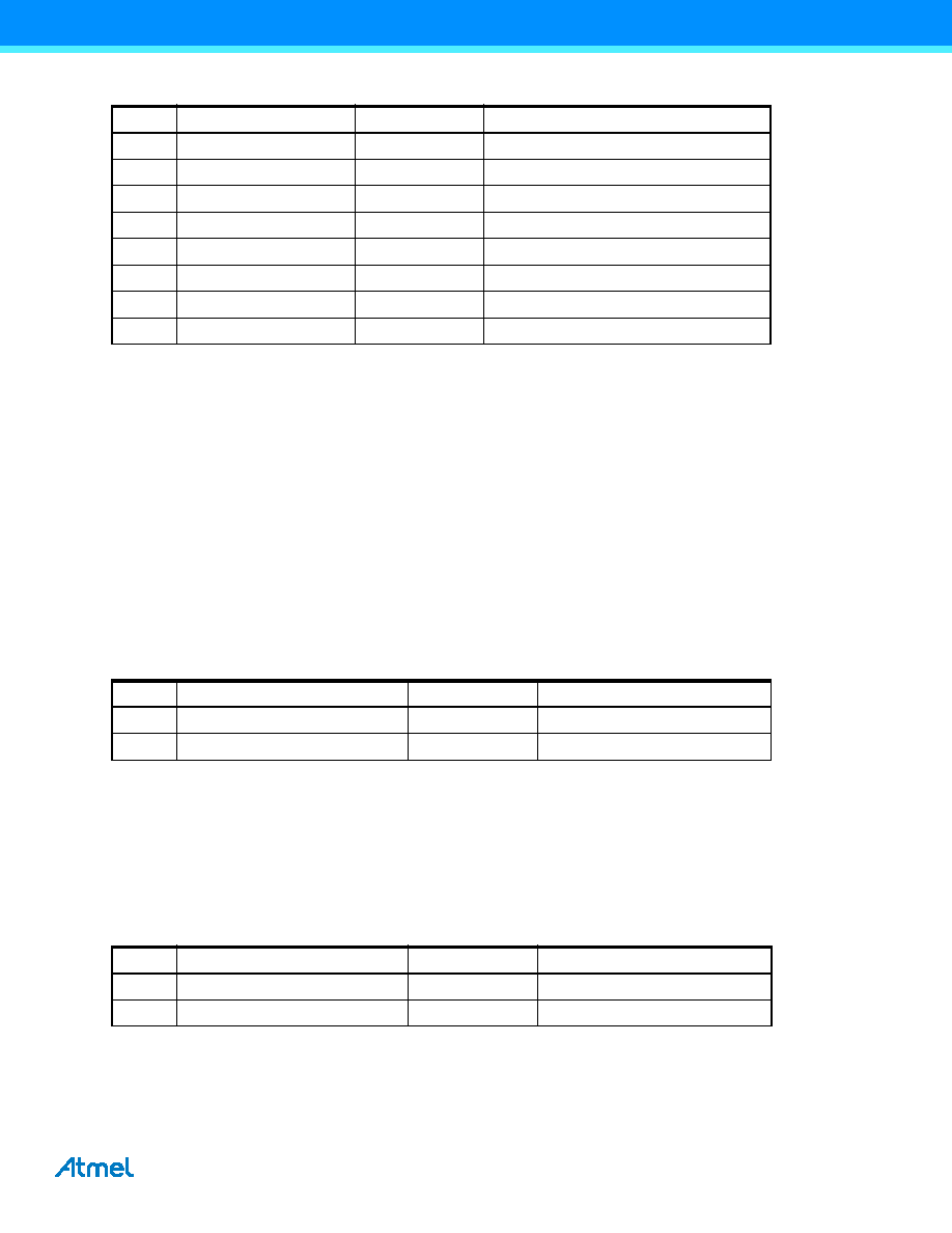
n
Write handshaking
ADDR0
Memory Address LSB
n+1
Write handshaking
ADDR1
Memory Address
n+2
Write handshaking
ADDR2
Memory Address
n+3
Write handshaking
ADDR3
Memory Address
n+4
Write handshaking
DATA
*Memory Address++
n+5
Write handshaking
DATA
*Memory Address++
...
Table 20-9.
Write Command (Continued)
Step
Handshake Sequence
MODE[3:0]
DATA[7:0]
Table 20-10. Full Erase Command
Step
Handshake Sequence
MODE[3:0]
DATA[15:0] or DATA[7:0]
1
Write handshaking
CMDE
EA
2
Write handshaking
DATA
0
Table 20-11. Set and Clear Lock Bit Command
Step
Handshake Sequence
MODE[3:0]
DATA[15:0] or DATA[7:0]
1
Write handshaking
CMDE
SLB or CLB
2
Write handshaking
DATA
Bit Mask
发布紧急采购,3分钟左右您将得到回复。
相关PDF资料
TS87C54X2-LIC
IC MCU 8BIT 16K OTP 30MHZ 44PQFP
TS87C54X2-VIC
IC MCU 8BIT 16K OTP 40MHZ 44PQFP
PIC24FJ64GB002-I/SP
IC MCU 16BIT 64KB FLASH 28DIP
PIC24FJ128GA306-I/PT
MCU 16BIT 128KB FLASH 64TQFP
TS87C54X2-LCE
IC MCU 8BIT 16K OTP 30MHZ 44VQFP
TS80C51RA2-LCE
IC MCU 8BIT 256BYTE 30MHZ 44VQFP
TS87C51RD2-VCE
IC MCU 8BIT 64K OTP 40MHZ 44VQFP
TS87C54X2-LIE
IC MCU 8BIT 16K OTP 30MHZ 44VQFP
相关代理商/技术参数
PIC16C63A-20E/SO
功能描述:8位微控制器 -MCU 7KB 192 RAM 22 I/O RoHS:否 制造商:Silicon Labs 核心:8051 处理器系列:C8051F39x 数据总线宽度:8 bit 最大时钟频率:50 MHz 程序存储器大小:16 KB 数据 RAM 大小:1 KB 片上 ADC:Yes 工作电源电压:1.8 V to 3.6 V 工作温度范围:- 40 C to + 105 C 封装 / 箱体:QFN-20 安装风格:SMD/SMT
PIC16C63A-20E/SP
功能描述:8位微控制器 -MCU 7KB 192 RAM 22 I/O RoHS:否 制造商:Silicon Labs 核心:8051 处理器系列:C8051F39x 数据总线宽度:8 bit 最大时钟频率:50 MHz 程序存储器大小:16 KB 数据 RAM 大小:1 KB 片上 ADC:Yes 工作电源电压:1.8 V to 3.6 V 工作温度范围:- 40 C to + 105 C 封装 / 箱体:QFN-20 安装风格:SMD/SMT
PIC16C63A-20E/SS
功能描述:8位微控制器 -MCU 7KB 192 RAM 22 I/O RoHS:否 制造商:Silicon Labs 核心:8051 处理器系列:C8051F39x 数据总线宽度:8 bit 最大时钟频率:50 MHz 程序存储器大小:16 KB 数据 RAM 大小:1 KB 片上 ADC:Yes 工作电源电压:1.8 V to 3.6 V 工作温度范围:- 40 C to + 105 C 封装 / 箱体:QFN-20 安装风格:SMD/SMT
PIC16C63A-20I/ML
功能描述:8位微控制器 -MCU 7KB 192 RAM 22 I/O RoHS:否 制造商:Silicon Labs 核心:8051 处理器系列:C8051F39x 数据总线宽度:8 bit 最大时钟频率:50 MHz 程序存储器大小:16 KB 数据 RAM 大小:1 KB 片上 ADC:Yes 工作电源电压:1.8 V to 3.6 V 工作温度范围:- 40 C to + 105 C 封装 / 箱体:QFN-20 安装风格:SMD/SMT
PIC16C63A-20I/SO
功能描述:8位微控制器 -MCU 7KB 192 RAM 22 I/O RoHS:否 制造商:Silicon Labs 核心:8051 处理器系列:C8051F39x 数据总线宽度:8 bit 最大时钟频率:50 MHz 程序存储器大小:16 KB 数据 RAM 大小:1 KB 片上 ADC:Yes 工作电源电压:1.8 V to 3.6 V 工作温度范围:- 40 C to + 105 C 封装 / 箱体:QFN-20 安装风格:SMD/SMT
PIC16C63A-20I/SO
制造商:Microchip Technology Inc 功能描述:8BIT CMOS MCU SMD 16C63 SOIC28
PIC16C63A-20I/SP
功能描述:8位微控制器 -MCU 7KB 192 RAM 22 I/O RoHS:否 制造商:Silicon Labs 核心:8051 处理器系列:C8051F39x 数据总线宽度:8 bit 最大时钟频率:50 MHz 程序存储器大小:16 KB 数据 RAM 大小:1 KB 片上 ADC:Yes 工作电源电压:1.8 V to 3.6 V 工作温度范围:- 40 C to + 105 C 封装 / 箱体:QFN-20 安装风格:SMD/SMT
PIC16C63A-20I/SP
制造商:Microchip Technology Inc 功能描述:IC 8BIT CMOS MCU 16C63 SDIL28